
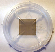
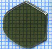
Monolayer Graphene Films on SiC
Nitride Crystals, Inc. is a supplier of high-quality epitaxial graphene films on silicon carbide (SiC) wafers for commercial use. Our graphene films on SiC are manufactured using the progressive technology of thermal decomposition of silicon carbide. Our graphene's excellent properties make it a promising material for various electronic applications and sensors.
Nitride Crystals currently offers epitaxial graphene films on conductive and semi-insulating 4H-SiC wafers.

- Single crystal
- C-Plane 15mm and 2"
- M-Plane 15mm
- High UV transparency
- High resistivity
Substrates for Nitride Devices
Nitride Crystals, Inc. manufactures substrates for a broad range of III-nitride devices. These include single-crystal AlN substrates and SiC Lely crystals in a variety of difficult-to-find polytypes for the researcher interested in exploring the behavior of various SiC polytypes.
The single-crystal AlN substrates are available in 15mM and 2” diameter for C-Plane polar orientation and 15mM diameter M-Plane non-polar orientation. On special order, other orientations of single crystal AlN substrates can also be produced. Aluminum Nitride wafers can be regarded as the universal native substrate for the growth of III-nitrides.
Nitride Crystals, Inc. has available a stock of high-quality Lely crystals of various polytypes. The supply of the more rare polytypes is limited; however, they offer an opportunity for scientists to explore the properties of SiC polytypes that are not commonly available.
Graphene on SiC
There are different methods of obtaining graphene, which can be divided into several main groups: mechanical methods, chemical methods, methods of growth on different wafers, and the method of thermal decomposition of SiC. The method of mechanical exfoliation was developed by A. Geim and K. Novoselov. They initially used an adhesive tape to pull graphene sheets away from graphite. Achieving monolayer graphene typically requires multiple exfoliation steps. The exfoliation method has no analogs forthe manufacture of large size (up to ~1 mm) samples suitable for transport and optical measurements.
The method of chemical intercalation consists of the intercalation of graphite by acids with the subsequent ultrasonic splitting. This method is characterized by a large material output, however, a small size of the obtained films (~10-1000 nm). Another disadvantage of the method is the destruction of the crystalline lattice of graphene, leading to a considerable degradation of its electric properties. The most perspective methods of graphene manufacture from the point of view of industrial application are chemical vapor deposition (CVD) and thermal decomposition of SiC.
Chemical vapor deposition is a rather cheap and easy method of obtaining graphene of relatively high quality. Graphene films are mostly deposited to surfaces of metals, such as Ni, Pd, Ru, Ir, Cu and others. Today, large size polycrystalline graphene films can be grown by CVD. The advantage of this method is the scalability of the obtained samples. Difficulties of the CVD method relate to controlling monolayer growth as well as the possibility of defects in the resulting material. At present, the majority of manufacturers of graphene films for industrial applications use this technique.
We have developed a technology for the growth of graphene films on SiC wafers by thermal decomposition of the SiC surface in argon ambient. This technology can be used for the production of gas sensors and bio sensors. The main advantages of growing graphene films on silicon carbide include:
- The possibility of obtaining large-size graphene films. Graphene films can be grown on an area as large as the SiC wafer. At present wafers up to 6 inch (150 mm) are available commercially.
- The ability to grow graphene on insulating silicon carbide wafers, which is essential to eliminating the effect of conductivity on the characteristics of graphene devices.
- Silicon carbide wafers available today offer high structural perfection and low dislocation density, that have a positive effect on the graphene quality.